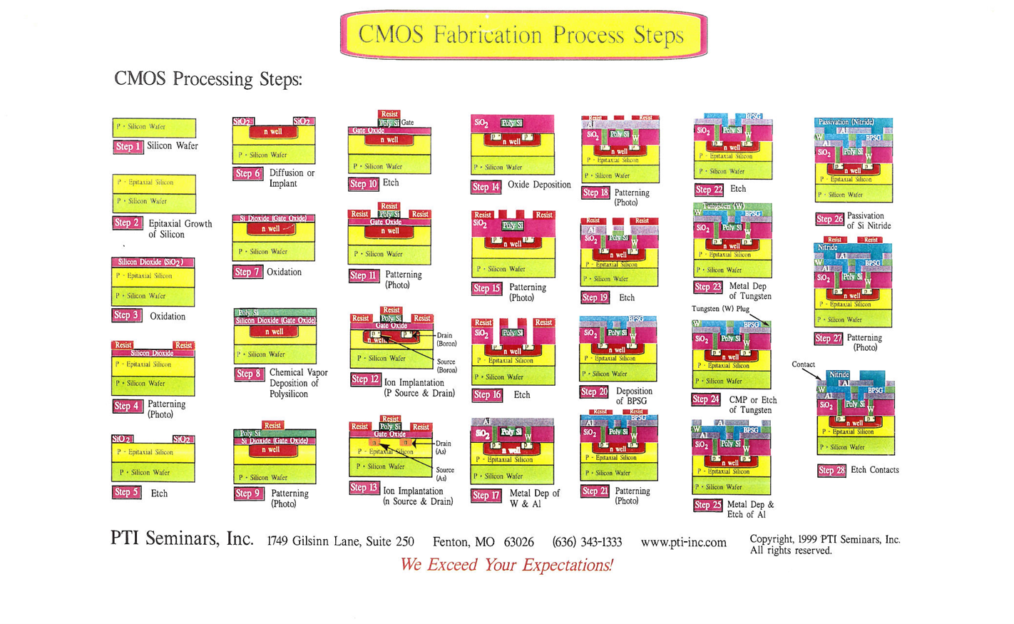
生产
横截面 cross-section
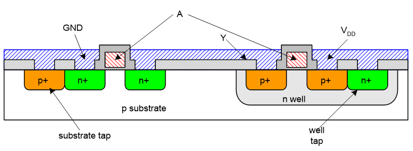
掩 mask-set
流程
新方法:放倒
管特性
三种工作
- cutoff
- linear
- saturation
电路设计
设计原则
- Complementary互补的
- 电阻匹配
- 不用DLD算,而是直接分配,能省管
- nmos一定要接地,pmos接VDD(因为否则导通后VGS不满足VT)
常见电路
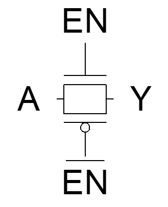
Tristates
- pass-transistor
设计简单,元件少,但是A的噪声会传递到Y
- Tri-state inverter
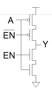
反相器,但是噪声小
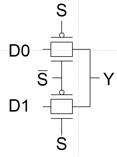
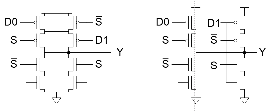
Multiplexers
D Latch
Flip-flop
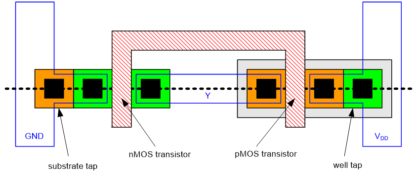
布局设计
根据图纸数尺寸
- Feature size f : distance between source and drain
- λ = f/2
反相器例子
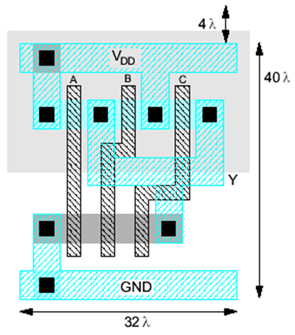
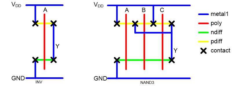
要会画stick diagram
要会数多少个λ
反相器
在 $\beta_p/\beta_n=1$ 时
| Region | nMOS | pMOS |
|---|---|---|
| A | Cutoff | Linear |
| B | Saturation | Linear |
| C | Saturation | Saturation |
| D | Linear | Saturation |
| E | Linear | Cutoff |
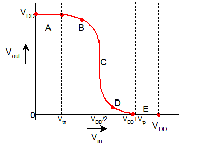
若 $\beta_p/\beta_n > 1$ 称为p strong,C点会向右偏移,需要更高压才能关闭p,反之亦然。
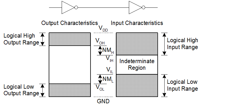
noise margins
计算延迟
认识参数
| 意义 | 计算 | |
|---|---|---|
| $t_{pdr}$ | rising propagation delay | From input to rising output crossing VDD/2 |
| $t_{pdf}$ | falling propagation delay | From input to falling output crossing VDD/2 |
| $t_{pd}$ | average propagation delay | (tpdr+tpdf)/2 |
| $t_r$ | rise time | From output crossing 0.2 VDD to 0.8 VDD |
| $t_f$ | fall time | From output crossing 0.8 VDD to 0.2 VDD |
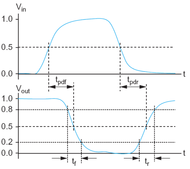
| 意义 | 计算 | |
|---|---|---|
| $t_{cdr}$ | rising contamination delay | From input to rising output crossing VDD/2 |
| $t_{cdf}$ | falling contamination delay | From input to falling output crossing VDD/2 |
contamination delay和propagation delay都是输入到输出的延迟,不同点在于不同输入情况,延迟不同。
RC Delay Model
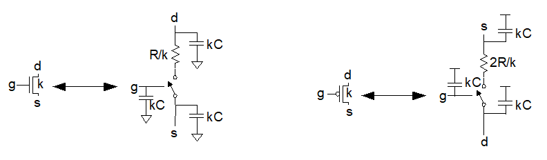
example1
example2
分析不同情况看谁在给谁充放电
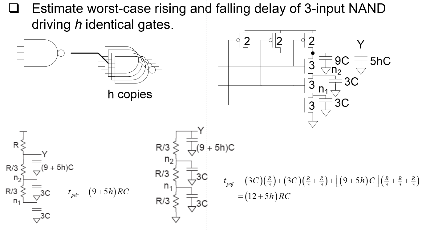
其中:9RC或12RC是Parasitic delay;5hRC是Effort delay
左图是111->011; 右图是000->111
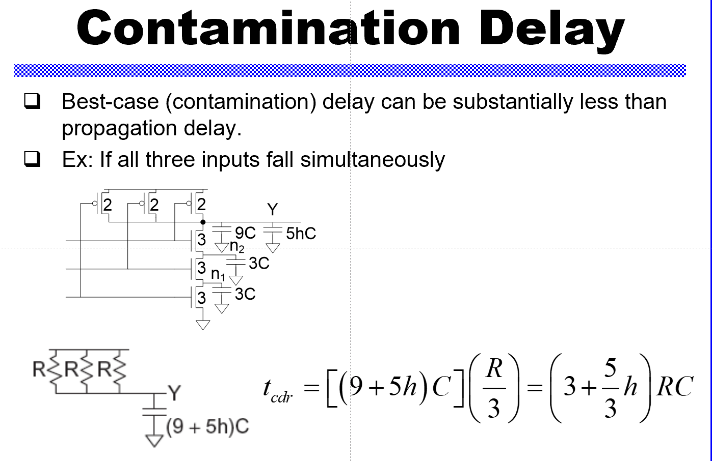
上图是111->000
diffusion capacitance
合理的设计,可以合并电容
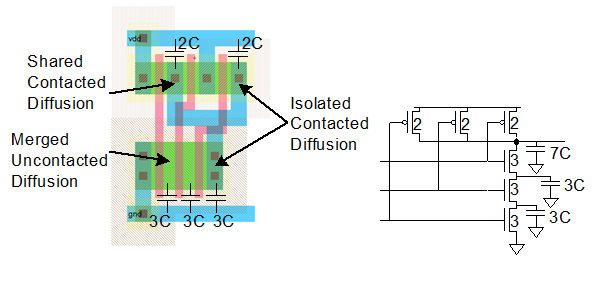
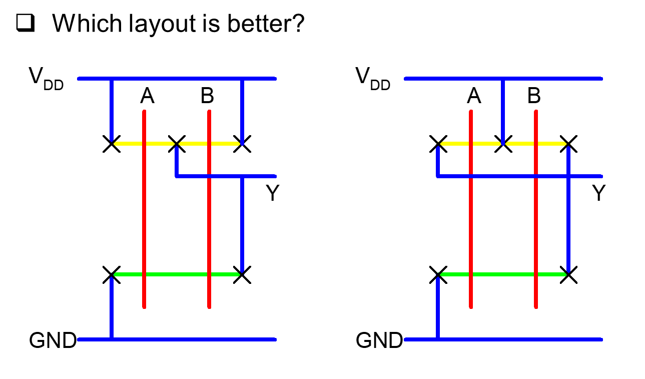
左边好,所以尽量接电源或者地,级连在一起
门电路延迟
- d: delay
- f: effort delay (stage effort)
- p: parasitic delay (Represents delay of gate driving no load)
- g: logical effort (Measures relative ability of gate to deliver current)
- h: electrical effort (Ratio of output to input capacitance)
g
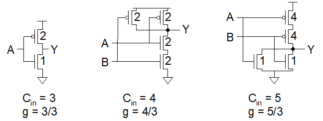
| 1 | 2 | 3 | |
|---|---|---|---|
| Complementary(串联相加,并联不用管,系数除,pmos乘2) | 2/2 = 1 | 2/2 = 1/2 + 1/2 | 2/4 + 2/4 = 1 |
| Cin(nmos系数+pmos系数) | 1+2 | 2+2 | 1+4 |
| g(nmos系数+pmos系数,除以3) | (1+2)/3 | (2+2)/3 | (1+4)/3 |
p
门电路输入个数
h
输出fan-out比输入fan-in
与个数有关,也与门电路上的数字有关
如果最后是一个电容,上面的数字也一样
门电路multistage延迟
effort
- F:path effort
- B:路线个数
delay
- D: Path Delay
- D_F: Path Effort Delay
- P: Path Parasitic Delay
design fast circuits
Delay is smallest when each stage bears same effort
- N: stage, 信号要通过几层门电路
work backward
example
找Best Stage Effort
F和N满足什么关系时,D最小
$\hat{f}=F^{1\over N}$=3.59 (for p = 1)
所以尽量凑4
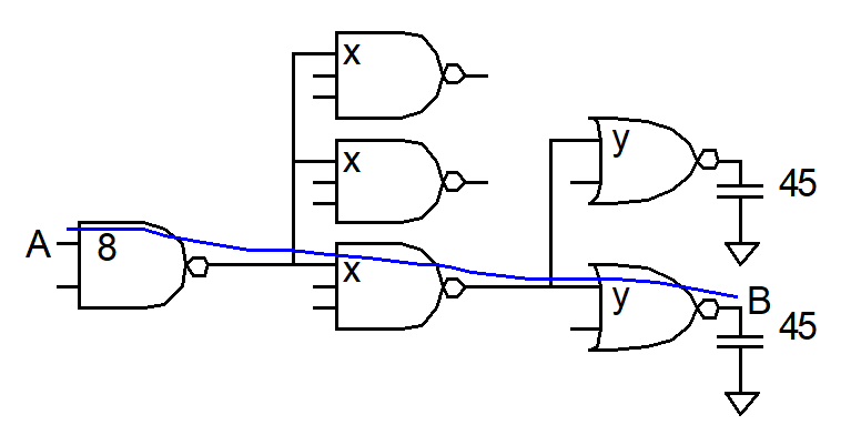
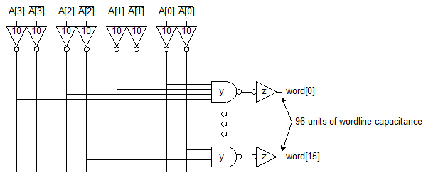
example解码器4输入16输出

B:对于每根线,要输出到16输出中的8个输出(因为一半需要反向的,暂不考虑)
H:在这8个输出中,每个输出有32bit宽度?每个bit又能驱动3个单位管。输入是每根线能驱动10单位管
G:暂定为1
算F,算N=3.1
根据3个stage设计电路
重新算F。。。
计算功耗
- Activity factor
- Capacitance
- Supply voltage
- Frequency
算prob
wires
R=rou/t*l/w=R.l/w
lec11:那几个定义,那几个公式
latch 设计
直接一个管
Vt drop
无法存储
backdriving
output noise sensitivity
俩管对着
无法存储
backdriving
output noise sensitivity
加inverter
- 无法存储
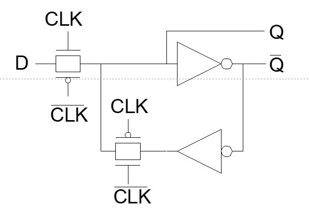
最终形态

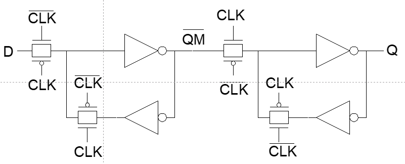
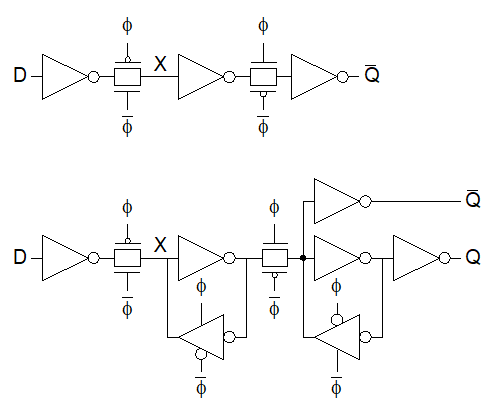
flip-flop 设计
Pitfall
qVariation
qNoise Budgets
qReliability
qCircuit Pitfalls
测试 test
test
Logic Verification
Silicon Debug
检测有没有设计不合规的qelectrical failures
用Shmoo Plots(用不同的电压、频率,在失败的地方画点)

Manufacturing Test
Fault Models
Stuck-At Faults
假设错误只有短接地或电源
测试思路
每个输入变量挨个测试。对每个输入变量,找一组输入,满足改变该变量,输出会改变。把所有组合找不重复集合。
测试方法
scan
在设计芯片的时候就在每个口留个测试通道——复用器,选择测试或正常运算。
测试通道首尾相俩,测试的时候就从上向下shift传进去
ATPG
- PRSG
- BILBO
多想多做,发篇一作